Our customers often ask how thick copper can they use on their boards. For us, as a PCB manufacturer would be best to produce two different boards: one for signal part and second for power part of the design. For the signal part we could use thinner copper foil and for power part thicker. But this is usually not the case and brings the question how thick copper should I use so the board is producible. It is necessary to understand how PCBs are made and what the risks when using thick copper foil are. It is not only under-etching of the wire, but also about total balance of design with regards to galvanic process. It is impossible for any galvanic process to plate well boards that have large copper areas on one side and fine micro wires on second side.
| Thickness of Cu foil |
Wire width, annular ring ( driller / pad) |
Isolation gap |
Under-etching |
| 9µm |
0,10mm |
0,10mm |
20µm |
| 18µm |
0,12mm |
0,12mm |
30µm |
| 35µm |
0,20mm |
0,15mm |
40µm |
| 50µm |
0,25mm |
0,20mm |
50µm |
| 70µm |
0,30mm |
0,20mm |
70µm |
| 105µm |
0,35mm |
0,20mm |
105µm |
- values in table are the lowest possible. The higher the values are, the better.
Other possibilities can be consulted with our technicians.
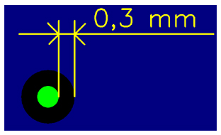
| - for the inner layers of multilayer printed circuit board is important to keep a minimum distance from the edge of the hole to the first object nearest 0.3 mm !! (Drill diameter is 0.1 mm larger than the hole in the final design of the system) |
|


 company adress :
 place of business :