H.A.S.L. Hot Air Solder Leveling
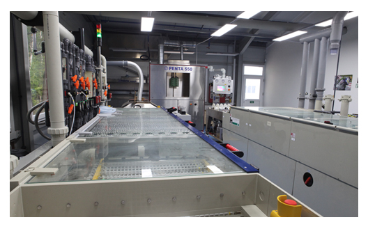 |
H.A.L. is the basic surface working of printed circuits boards. A pre-treated board is dipped into molten Sn solder ( since 1.7.2006 unleaded technology ) and after it comes out, the excess tin is removed by a hot air knife. Currently this technology is being substituted by other higher quality methods of surface working (chemical tin, chemical gold......). |
benefits : easy solderability, high throughput workplace, Ge (Germanium) reduces the surface tension of the molten solder and thus improves the wetting properties, reduces the development of micro cracks
disadvantages : energy consumption of operation, defective of surface flatness
used lead-free solder composition Felder Sn100Ni+ : Sn99,3Cu0,7NiGe  Technical specification - Felder SN100Ni+
Immersion tin plating
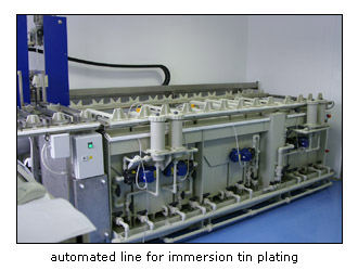 |
Due to the necessity to convert some technologies into an unleaded version and because of introducing new technologies, we acquired a new automated line for immersion tin plating etc. with the process CSN-FF-W from the company Ormecon in March 2006. The system is great at stability of parameters, excellent solderability and long-term storability. It does not erode the surface of non-soldering mask and it is ideal for fine pattern structures and for flexible printed circuits. Owing to the low operating temperature, it reduces tortuosity and expansivity of the material. Moreover, this system excels at reducing the formation of tin protuberances. The hanging baskets designed by us facilitate high passability and high-quality processing of boards in all baths including rinsing. |
Chemical gold plating
OMG™ Fidelity Electroless Nickel / Immersion Gold
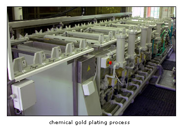 |
OMG™ Fidelity has long been a recognized leader with ENIG for many different applications including hard disk drives, plating on plastics and electronics finishing. With the development of electroless nickel and immersion gold, Fidelity has risen to the challenges and demands faced by fabricators, OEMs and assemblers worldwide. The Fidelity Electroless Nickel Process provides maximum uniformity of deposit and unsurpassed stability. The tight-grained nickel structure insures maximum corrosion resistance and helps to reduce the incidence of black pad. Smooth nickel deposit promotes uniform tin-nickel intermetallic-thus improving joint reliability.
|
Inner layer black oxidizing
 The new and simple system Atotech BondFilm was developed so that it could substitute standard industrial process with copper oxide, which has been used so far to produce high-quality multi-layered connections. By means of the BondFilm, an even, brown, metalorganic layer on the copper surface is produced. Thus an increased firmness between inside layers and plastic fabric is guaranteed in production of multi-layered printed circuits. The requirements concerning thinner materials, finer lines and smaller holes have continually increased because of the demands for up-to-date technological procedures. The oxide procedure is no exception. The complexity of the connecting process is increased by blind holes, blind holes (connecting holes of inside layers) and covered holes. The aim of the industry to reduce prices, simplify the waste treatment and increase productivity with improved quality, especially in the horizontal technique, contributes to this development. These constantly increasing higher requirements which make demands on the producers of printed circuits, together with significant increase of application of direct metallizing, brought the common oxide procedures to its technical limits. Nevertheless, Atotech developed the procedure BondFilm-process, so that it could substitute the common oxide technologies and improve them in addition. Moreover, a special accent is put on a higher asserted amount in horizontal technique with concurrent improvement of the quality of inside layers. In connection with the horizontal technique from the Atotech, the BondFilm offers the producers of printed circuits the best solution to this problem available in contemporary trade.
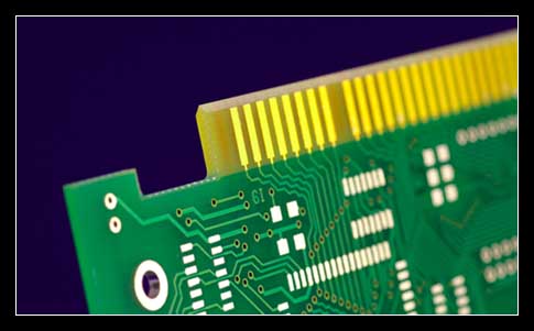
Hard gold plating
With the direct plating of connectors is used by the galvanic process Ni/Au metallization with the thickness 5/1μm. For special orders it is possible to use the hard metal golding the entire surface (rather than as a resist galvanic tin). The level of full-scale gold consult you, please, with the receipt of orders technicians. Of course there is a direct plug chamfer angle of 45 ° or other.

 company adress :
 place of business :